
Key Takeaways:
- The embedded product development life cycle is the full journey a hardware-plus-software product takes from an idea to a shipped, supported device.
- It is really two tracks, hardware and firmware, running side by side and meeting at integration.
- A typical project takes 4 to 12 months from requirements to a production-ready design, and longer for regulated products.
- The process loops back on itself more often than most guides admit, and the projects that go wrong usually skip requirements, lose track of handoffs, or rush into manufacturing without a proper test gate.
Most guides to embedded product development show a neat row of four boxes: plan, design, build, ship.
If you have ever actually run one of these projects, you know that is not how it goes.
- Hardware and firmware happen at the same time, not one after the other.
- A prototype reveals that a requirement was wrong and you go back two steps.
- A part goes out of stock and the schematic changes after the firmware was written against it.
This guide is the version we wish we had when we started. It covers every phase, explains how the hardware and firmware sides fit together, gives an honest answer to "how long does this take", and lists the ways these projects most often break down.
What Is the Embedded Product Development Life Cycle?
The embedded product development life cycle is the sequence of phases an embedded product moves through, from identifying a need, through requirements, design, prototyping, testing and manufacturing, to support and eventual retirement. Unlike a pure software lifecycle, it covers physical hardware and the firmware that runs on it, and the two are developed together.
The "software" in these devices is called firmware because it is written for that specific hardware and usually lives in the chip's memory permanently.
How is an Embedded Product Development Lifecycle Different From a Typical Software Product Lifecycle
If you come from a software background, two things will feel unfamiliar.
Hardware and firmware tracks run in parallel
Any firmware development company that’s worth its salt, will tell you that we cannot wait for the finished circuit board before starting the firmware. The board takes months and the firmware takes months, and doing them one after the other would double the schedule.
So firmware development starts on evaluation boards and development kits while the real board is still being designed. The two tracks meet when the first real boards arrive and the firmware is brought up on them.
A simple example: a team designing a battery-powered sensor starts firmware work on a vendor's development kit in month one. The custom board is designed in months one to three. In month four the first boards arrive, and the firmware that already works on the dev kit is ported and debugged on the real hardware.
That parallel structure is the single most important thing to understand about this lifecycle, and it is why we think of it as the Two-Track Lifecycle.
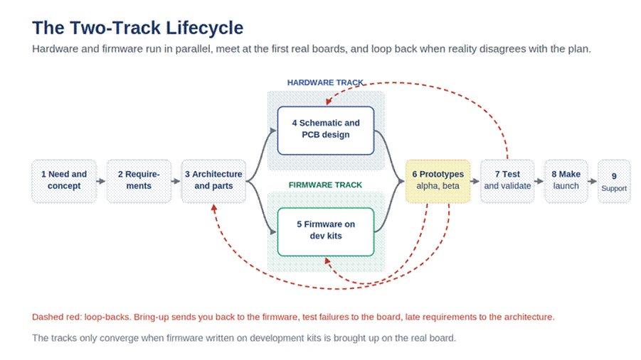
The Two-Track Lifecycle. The two tracks meet at the first real boards, and loops back are part of the plan.
Altext: The Two-Track Lifecycle
Embedded PDLCs are iterative, not linear
Every embedded project has moments where a later phase sends you back to an earlier one. The alpha prototype shows that the enclosure blocks the antenna, so the board layout changes. A component becomes unavailable, so the schematic changes and a driver has to be rewritten. A field trial reveals a requirement nobody wrote down.
None of this means the process failed. It means the process worked, because you found the problem before manufacturing. A realistic lifecycle plans for these loops instead of pretending they will not happen.
What the Two Tracks Look Like on a Real Project
A concrete example makes the parallel-track idea easier to picture. When LIFO built the automated LPG cylinder vending machines deployed by BPCL, the hardware track was designing the sensor and control electronics while the firmware track was writing the dispensing logic as a state machine on a development kit.
The two met at the alpha prototype, where every sensor reading that gates a dispensing step was tested on real hardware, then again on a hardware-in-the-loop rig that could simulate out-of-range readings safely.
Remote diagnostics were designed during the requirements phase, not added after launch, which is why operators can now see the health of every unit across multiple sites from one place. The loop-backs happened too: field trials sent the team back to the firmware for edge cases nobody had written down. That is the lifecycle working as intended.
Why Following the Full Embedded PDLC Matters
It is tempting to skip phases when the deadline is close. But following the full cycle makes you get four things right.
• Hardware mistakes stay cheap: A problem found at schematic review costs an afternoon. The same problem found after manufacturing costs a recall.
• The two tracks stay in sync: Phase gates force the hardware and firmware teams to agree on what exists before either moves on.
• Certification is designed in, not bolted on: Compliance targets set in the requirements phase shape the layout, the firmware and the test plan.
• The product can be supported: A documented lifecycle leaves behind the drawings, test results and update mechanisms the support team will need for years.
The Complete Embedded Product Development Life Cycle Explained: Stage by Stage
Here is the full Two-Track Lifecycle, phase by phase. Phases 4 and 5 run at the same time while everything else is roughly in order, with loops back where noted.
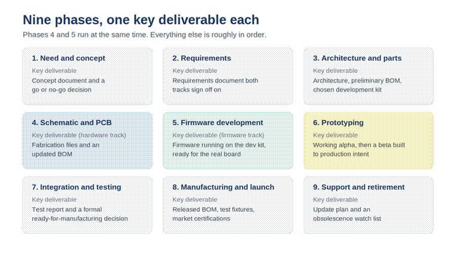
Nine phases, one key deliverable each. Phases 4 and 5 run at the same time.
Phase 1: Need and Concept
The work in this phase is turning a vague need into a concept proposal.
How it is done: The team writes a one-page problem statement describing who has the problem and how they cope with it today. They conduct interviews to check what already exists, both competing products and off-the-shelf modules. A senior engineer sketches one or two concept options as block diagrams, puts rough numbers on the best one, and the phase closes with a concept review and a decision.
Documents involved
- Problem statement
- Concept proposal of three to eight pages with the block diagram
- Target unit cost and volumes, the development cost and timeline ranges
- Assumptions behind them, and the top risks
- A short feasibility note for any serious technical unknown
- A decision record stating go, no-go, or go once a named risk is retired
Who is involved
- A product owner or sponsor owns the need and the budget.
- A senior embedded engineer or architect draws the block diagram, judges feasibility, and produces the rough costs.
- A Sales rep or a domain expert, who confirms the problem is real and worth paying to solve.
- On larger products, a manufacturing or supply-chain voice sanity-checks the unit cost.
What a successful Phase 1 looks like
Phase 1 ends with a written concept that someone outside the team could read and understand. The cost target and budget range have their assumptions stated. The two or three biggest unknowns are named, each with a plan to reduce it. The constraints that will shape every later phase are captured in writing: target price, battery life, operating environment, and regulatory category. The decision is clear, and a well-reasoned no-go counts as a success.
Typical duration: Two to four weeks.
Key deliverable: a short concept document and a go or no-go decision. Skipping this phase, or doing it in someone's head, is where a lot of later confusion starts.
Phase 2: Requirements and Target Audience
This is where you write down what the product must do (functional requirements) and how well it must do it (non-functional requirements: battery life, operating temperature, size, cost, regulatory targets). Requirements are the contract between the hardware and firmware tracks.
How it is done
The concept is turned into numbered requirements, one statement each, written so that each can be tested. They are split into functional requirements, which describe what the product does, and non-functional requirements, which describe how well it must do it.
The team identifies the users and the conditions of use, profiles the competing products, and confirms the regulatory category and the certifications it implies. The phase closes with a requirements review that both tracks attend, after which the baseline is frozen.
Documents involved
- Requirements specification in which every requirement has a unique ID and a priority.
- Description of the users and the environment the product will live in.
- List of the regulatory and compliance targets. A register of assumptions and open questions.
- Sign-off record from the hardware lead, the firmware lead and the product owner.
Who is involved
- The product owner owns the requirements and settles priorities when they conflict.
- The hardware lead and the firmware lead check that every requirement can be built and tested. A test engineer confirms that each one can be verified.
- A compliance adviser names the standards that apply.
- Where possible, a customer or someone from the field keeps the list honest.
What a successful Phase 2 looks like
Every requirement has an ID, a number where it needs one, and a way to test it. Both tracks have signed the same document. Non-functional targets such as battery life and temperature range are written down rather than assumed. The regulatory targets are known before anyone draws a schematic. Open questions are listed instead of being silently guessed.
Typical duration: Two to four weeks.
Key deliverable: A requirements document that both tracks sign off on.
Phase 3: System Architecture and Component Selection
In this phase, the team decides how the product gets built. The engineers decide which functions live in hardware and which in firmware, which processor family, whether it runs an RTOS or bare-metal code, and which sensors, radios and power components.
How it is done
The architect draws the system block diagram and decides what is done in hardware, firmware and higher-level software. The team chooses the processor family and the RTOS or bare-metal approach, then selects the major components against the requirements.
Every key part is checked for lifecycle status, lead time and the existence of a second source. Cost and power budgets are estimated, and a development kit is chosen so that firmware work can start straight away.
Documents involved:
- Architecture document with the block diagram and the hardware-firmware split.
- Preliminary bill of materials with a unit cost estimate.
- Component risk register covering obsolescence, lead times and single-source parts.
- Power budget, and a thermal estimate where heat matters.
- Interface control document that lists the pins, buses and signals the two tracks will share.
Who is involved
- A system architect or senior embedded engineer owns the architecture.
- The hardware engineer handles component selection, power and cost.
- The firmware lead chooses the processor, the RTOS approach and the development kit.
- Supply chain or procurement checks lead times, availability and second sources.
- The mechanical engineer contributes the enclosure constraints that shape the board.
What a successful Phase 3 looks like: The two tracks agree on an interface document before either of them starts. No key part is single-source or near end of life without a stated plan. The bill of materials meets the unit cost target with some margin. The power budget shows that the battery-life target is reachable. Firmware work can begin on a development kit the same week.
Typical duration: Two to four weeks.
Key deliverable
An architecture document, a preliminary bill of materials (BOM), and a chosen development kit so firmware work can start immediately.
Phase 4: Schematic and PCB Design (Hardware Track)
The hardware team turns the architecture into a schematic (the circuit diagram) and then a printed circuit board (PCB) layout. This phase runs at the same time as Phase 5.
How it is done
The hardware engineer captures the schematic and holds a review against the requirements, with the firmware lead in the room. The layout engineer then places the components and routes power and signals, paying attention to heat, signal quality, and antenna keep-out areas.
Design rule checks are run, and a design-for-manufacturability review is done with the board maker before the order goes in. Throughout, every pin change is recorded in the interface document and passed to the firmware team.
Documents involved
- Schematic and layout files, with version numbers that everyone refers to.
- Fabrication files such as Gerbers, drill files and the layer stack-up, plus assembly files including pick-and-place data.
- DRC and DFM reports.
- A test-point list and a bring-up plan for the first boards.
- An updated bill of materials and interface document.
Who is involved
- The hardware engineer owns the schematic and the reviews.
- A PCB layout engineer handles placement, routing and manufacturability.
- The firmware lead reviews the schematic for what the code will need, such as test points, debug headers and sensible pin choices.
- The mechanical engineer sets the board outline, mounting and connector positions.
- The board fabricator and assembler give DFM feedback and lead times.
What a successful Phase 4 looks like
The firmware team has reviewed the schematic and nothing about it surprises them. DRC and DFM are clean before the boards are ordered. Debug and test access are designed in rather than improvised later. Every pin change has reached the firmware team through the interface document. The first boards are ordered with a bring-up plan already written.
Typical duration: Six to ten weeks of design, then two to four weeks for fabrication and assembly.
Key deliverable
Fabrication files and an updated BOM.
Phase 5: Firmware and Software Development (Parallel Track)
While the board is being designed, the firmware team builds the software that will run on it, most of it on development kits that use the same processor as the final board.
How it is done: The toolchain, version control and automated builds are set up on the first day. The firmware lead defines the architecture: the layers, the tasks and how modules talk to each other. Engineers write the drivers, communication stacks and bootloader on the development kit, then build the application logic against the requirements, writing unit tests as they go. Board-specific code, such as pin maps and power sequencing, is kept in one place so that it is easy to change at bring-up.
Documents involved
- Firmware architecture document.
- Coding standard and a description of the test approach.
- Documentation for each driver and module, at least at header level.
- Design for the bootloader and the update mechanism.
- Traceability list showing which requirement each module satisfies.
Who is involved
- The firmware lead owns the architecture, the reviews and the integration.
- Firmware engineers write the drivers, stacks, application code and unit tests.
- The hardware engineer answers questions about parts and timing before the real board exists.
- A test engineer builds test harnesses alongside the code.
- The product owner settles priority calls when requirements conflict.
What a successful Phase 5 looks like: The firmware runs end to end on the development kit before the real board arrives. Every driver has a test that can be re-run on the real board in minutes. Board-specific code is isolated and small. The bootloader and update path exist in some form, even a basic one. Code reviews and automated builds are routine rather than a late addition.
Typical duration: Eight to sixteen weeks, running alongside Phase 4.
Key deliverable: firmware that runs on the dev kit and is ready to bring up on the real board.
Phase 6: Prototyping (Alpha and Beta)
The first real boards arrive, and the two tracks meet. An alpha prototype proves the design functions; a beta prototype is close to the final product in components, enclosure and software.
How it is done: The first boards are inspected and powered up carefully, checking supplies and clocks before any firmware is loaded. The firmware is brought up one peripheral at a time, and every difference from the development kit is logged. The alpha is run against the core requirements and every issue is recorded. The team then decides together which fixes need a board revision and which are firmware-only, builds the beta with production-intent parts and enclosure, and puts it in the hands of early users.
Documents involved:
- A bring-up log recording what worked, what did not, and why.
- An issue list with an owner for each item and its fix path, whether hardware, firmware or mechanical.
- Board revision notes and updated schematics where the layout changed.
- Alpha and beta test reports against the requirements.
- A summary of early-user feedback.
Who is involved:
- Hardware and firmware engineers work together, ideally at the same bench.
- A test engineer runs the requirements checks and keeps the issue list honest.
- The mechanical engineer checks enclosure fit, thermal behaviour, buttons and connectors.
- The product owner and a few early users judge whether the beta solves the problem.
- The assembler or contract manufacturer gives feedback on building it.
What a successful Phase 6 looks like: Bring-up takes days rather than weeks, because the interface document was kept current. Every issue has an owner and a fix path, and nobody is arguing about whose fault it is. The beta is built from the parts and enclosure that will ship. Early users have used it and their feedback is written down. The list of changes for the production board is agreed and short.
Typical duration: Four to eight weeks per prototype round, and there are usually two rounds.
Key deliverable
A working alpha, then a beta built to production intent, each with a list of the issues it exposed and how they were resolved.
Phase 7: Integration and Testing
Testing in embedded projects has layers, and it helps to name them.
• Unit testing checks individual firmware modules in isolation.
• Integration testing checks that modules work together and talk to the hardware correctly.
• Hardware-in-the-loop (HIL) testing connects the real board to a rig that simulates the outside world, so you can test scenarios that are hard or dangerous to create for real.
• System testing exercises the complete product against the requirements.
• Validation confirms the product does what the user actually needs, in conditions close to real use.
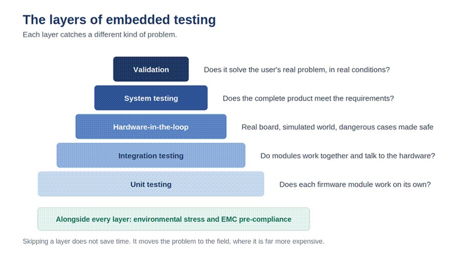
Alt text: Each testing layer catches a different kind of problem. Skipping one does not save time; it moves the problem to the field.
Environmental testing (heat, cold, humidity, vibration) and pre-compliance checks for electromagnetic emissions also belong here, before the formal certification submission.
Key deliverable: a test report showing which requirements passed, and a formal decision that the product is ready for manufacturing.
Phase 8: Manufacturing Transition and Commercial Launch
Moving from a few hand-built prototypes to hundreds or thousands of units is a project of its own, and compliance certification lands here too.
How it is done: The final bill of materials is released with approved suppliers and second sources. Production test fixtures are built to check every unit in seconds, and a factory test mode is added to the firmware. A pilot build is run with the contract manufacturer, and whatever the line finds is fixed. The product is submitted for formal certification, and the firmware release process, serial numbering, packaging and launch material are prepared in parallel.
Documents involved:
- The released bill of materials and the approved vendor list.
- Assembly drawings, work instructions and production test procedures.
- A pilot build report with yield and defects.
- Certification test reports and the certificates themselves.
- Release notes for the launch firmware and a procedure for updating units in the field.
Who is involved
- A manufacturing or production engineer owns the fixtures, work instructions and pilot build.
- The contract manufacturer handles assembly and reports yield and design feedback.
- Supply chain secures parts, lead times and pricing at volume.
- A compliance adviser and a certification lab handle submissions and reports.
- A firmware engineer delivers the factory test mode, the release build and the update mechanism.
- The product owner and sales set launch timing and line up the first customers.
What a successful Phase 8 looks like: The pilot build yield is high and every defect has a root cause. Every unit leaving the line has passed an automated test and carries a serial number. Certificates are in hand before the first customer shipment. Devices in the field can be updated without a site visit. The factory can build the product without calling the design team.
Typical duration: Eight to sixteen weeks to the first production run. Certification runs alongside and can take four to twelve weeks.
Key deliverable
A released BOM with approved suppliers, production test fixtures, and the certifications required for the target markets.
Phase 9: Support, Maintenance and Retirement
The product is in the field, and now the work changes shape: firmware updates, occasional hardware revisions as parts go obsolete, and learning from how the product is actually used.
How it is done: Field data and support tickets are collected and sorted into bugs, feature requests and misuse. Firmware updates ship on a planned cadence, over the air where possible, always with a way to roll back. The component watch list is reviewed regularly so that small hardware revisions can be planned before parts disappear. What the field teaches feeds the requirements for the next version. Eventually, an end-of-life date is set, customers are told early, and their migration is planned.
Documents involved:
- A support and update plan that states how long each version is maintained.
- Release notes for every firmware version.
- A component obsolescence watch list with the planned revisions.
- A field-issue log with root-cause records.
- An end-of-life notice and a customer migration plan.
Who is involved
- Support or customer success is the first contact and triages tickets.
- A sustaining firmware engineer handles updates, fixes and release management.
- The hardware engineer manages obsolescence revisions and re-qualification.
- Supply chain arranges last-time buys and second sources.
- The product owner sets the roadmap for the next version and makes the retirement decision.
What a successful Phase 9 looks like: Field issues are traced to root causes and fixed in a release rather than patched one unit at a time. No part goes obsolete without warning, because the watch list is kept. Updates reach the fleet without site visits and can be rolled back if needed. The next version's requirements are shaped by real field data. Retirement is announced with enough time for customers to move.
Typical duration: The life of the product, which is commonly five to ten years for industrial devices.
Key deliverable: a support and update plan, and a watch list of components at risk of going obsolete.
How Long Does the Embedded Product Development Life Cycle Take?
A typical embedded product takes 4 to 12 months from requirements to a production-ready design, based on ranges reported by embedded services firms. Simple devices with off-the-shelf modules sit at the low end. Products with custom radio design, safety certification, or medical or automotive compliance often take 12 to 24 months, mainly because of certification and validation cycles.
Factors that stretch the timeline:
• Custom RF (wireless) design, which needs specialist layout and certification testing.
• Safety-critical or regulated categories, where documentation and validation are formal and slow.
• Long-lead components, where a single part can add months of waiting.
• Multiple prototype rounds, which are normal, but each board spin adds several weeks.
• Late requirement changes, which ripple through both tracks.
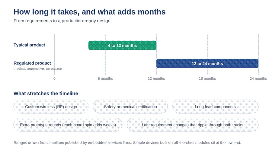
Where the months go, and what adds more of them.
Common Reasons Embedded Product Lifecycles Break Down
We have seen the same patterns cause trouble often enough that they are worth listing plainly.
Requirements were skipped or rushed: The team started designing with a rough idea, and the hardware and firmware sides quietly diverged. This is the most common root cause of late surprises.
Handoffs were undocumented: The hardware team changed a pin assignment and told the firmware team in a chat message that got lost. Weeks later, bring-up fails. Interface documents between the two tracks are boring and essential.
The lifecycle was treated as linear: The plan had no room for a second board spin, so the first loop-back blew the schedule and the budget.
There was no formal test gate before manufacturing: The prototype "mostly worked", and the pressure to ship pushed it into production with known issues. Fixing a firmware bug in the field is expensive; fixing a hardware bug in the field means a recall.
Compliance was considered at the end: A product designed without thinking about emissions testing can fail certification and need a layout change at the worst possible moment.
Component risk was ignored: A part with a single supplier went end-of-life, and a redesign followed.
How LIFO Helps With Embedded Product Development Lifecycle
Every one of the aforementioned reasons is avoidable, and most of them are avoided by the same thing: a lightweight but real process with clear phase gates, and a team that has run the whole cycle before.
The embedded product development life cycle is not four tidy steps. It is two tracks, hardware and firmware, running in parallel, converging at integration, and looping back whenever reality disagrees with the plan. Teams that plan for that reality ship on time. Teams that plan for the tidy version discover the loops anyway, just later and more expensively.
If you are mapping out your own process, use the nine phases above as a checklist and look for the gates you are missing. And if you would rather work with a team that has run both tracks together many times, LIFO's embedded engineering services cover the full cycle.
FAQ
What is the embedded product development life cycle?
It is the complete process an embedded product goes through: identifying a need, defining requirements, designing the architecture, developing hardware and firmware in parallel, prototyping, testing, moving to manufacturing, and supporting the product after launch.
What are the stages of embedded product development?
In this guide, nine stages: need and concept, requirements, architecture and component selection, schematic and PCB design, firmware development, prototyping, integration and testing, manufacturing transition and launch, and support and retirement. Other guides group them into four or five; the underlying work is the same.
How long does embedded product development take?
Typically 4 to 12 months to a production-ready design for a moderately complex product, and 12 to 24 months for products that need custom wireless design or safety, medical, or automotive certification.
What is EDLC (Embedded Development Life Cycle)?
EDLC is another name for the same thing. Some sources use it to mean the software side only; we use "embedded product development life cycle" to make clear that hardware is included.
Why is a structured lifecycle important for embedded products?
Because hardware mistakes are expensive to fix after manufacturing, and because two teams working in parallel need agreed checkpoints. A structured lifecycle is how you catch problems while they are still cheap.
What is the difference between embedded system design and general product development?
Embedded design combines custom electronics and firmware, so it has two parallel tracks, physical prototyping cycles, and certification requirements that pure software or pure mechanical products do not.
What is the difference between an alpha and a beta prototype?
An alpha prototype proves the design works and is expected to be rough. A beta prototype is close to the final product in components, enclosure, and software, and is used for early user trials and pre-compliance testing.
Do all embedded products need compliance certification?
Almost every product sold commercially needs some certification, at minimum for electromagnetic emissions and electrical safety in the markets where it is sold. Safety-critical, medical, and automotive products need additional, more demanding standards.